Introduction #
One of the devices that I recently received for tearing down was a Google Home Mini (first generation). This device was a home “assistant” that was released in late 2017. Unfortunately for me, this device has been torn down many, many times. If I want to get anything interesting out of it, I will need to do something past the regular disassembly and major circuit analysis. I can’t even contribute to a flash dump analysis without running into some work you can find on ArXiv.
One thing that I haven’t been able to see is any clone of the internal electronics. One of the tear downs mentioned that the boards are only two layers so they should make very good specimens for recreating in KiCad. In this post I walk through the reverse engineering of the input PCBA that houses the USB connector, microphone mute switch, factory reset switch, and connector the main PCB.
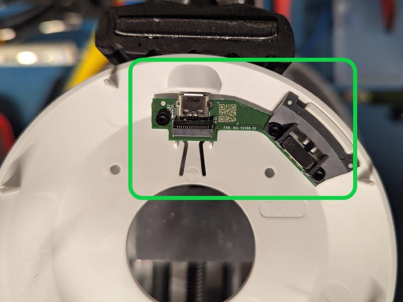
Reverse Engineering #
The steps in reversing this PCB should have been
- Take images of both sides
- Measure connector dimensions on board (especially height off PCB)
- Measure capacitance on board with a LCR
- Remove parts (save for later measurements)
- Use solder wick to remove as much solder as possible and flatten PCB
- Scan both sides of PCB with a printer
- Measure removed parts and identify alternatives available in distribution
- Input data into KiCad to redraw schematic and PCB
I made two mistakes on this first approach - I tried to measure the single capacitor off of the board and my spring probes launched it into oblivion and I melted the FFC connector and it snapped in half during disassembly. Luckily, going into this I will just guess 100nF for the capacitor and I was able to salvage enough of the FFC to identify a replacement.
Part Identification #
My process for identifying parts was to go to Digikey and start filtering down their catalog until there were only a few plausible options. For example, on the slide switch I went to:
- Digikey -> Switches -> Slide Switches
- In Stock
- C&K Manufacturer (marks were visible on the removed switch)
- SMD Right Angle Packages
- Actuator Length 2mm (I measured 2.09 with calipers)
At this point there was only 7 parts available and I could look through pictures and datasheets to find what appears to be the closest match.
Repeating this process for all of the parts (except for the capacitor which I launched across the room), I was able to come up with this BOM).
| Reference | Manufacturer | Manufacturer PN |
|---|---|---|
| J1 | Molex | 475900001 |
| J3 | Hirose | FH34SRJ-16S-0.5SH(99) |
| SW1 | Alps Alpine | SKSGACE010 |
| SW2 | C&K | JS102011JAQN |
PCB Layout #
For the PCB Layout, I placed “Reference Images” in KiCad. The scans were taken at the highest DPI I can achieve with my scanner (600), cropped down, and then rotated to try and keep have the straight edges along the X-axis.
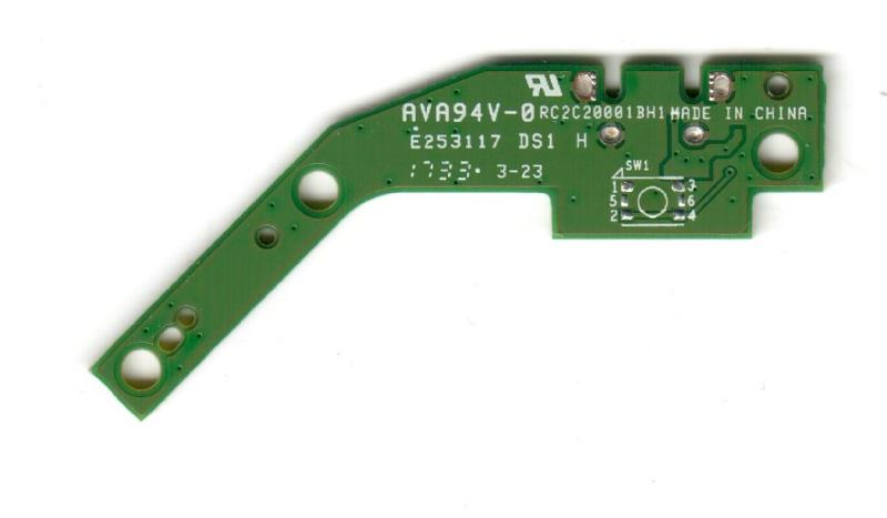
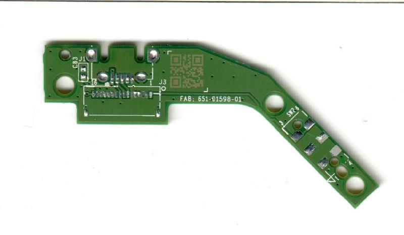
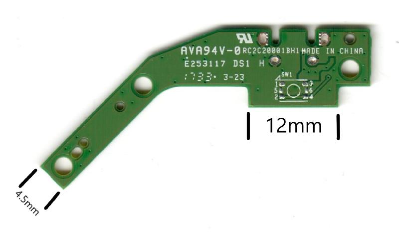
When KiCAD imports these images they do not come in scaled correctly so I had to choose a few measurements to match up and rescale the image. For this I primarily looked at the longest straight line on a regular axis and lined up the 12mm edge shown below.
The next challenge in getting the reference images in KiCAD is the vias. It is very difficult to get them to line exactly up, probably due to a slight tilt in one or both of the images. This tilt is potentially from the surfaces not being completely flat (solder on pads) or from the cover of the scanner pushing on the PCB and tilting it slightly. I was able to get them all within a few fractions of a mm, but it is still an issue to watch out for.
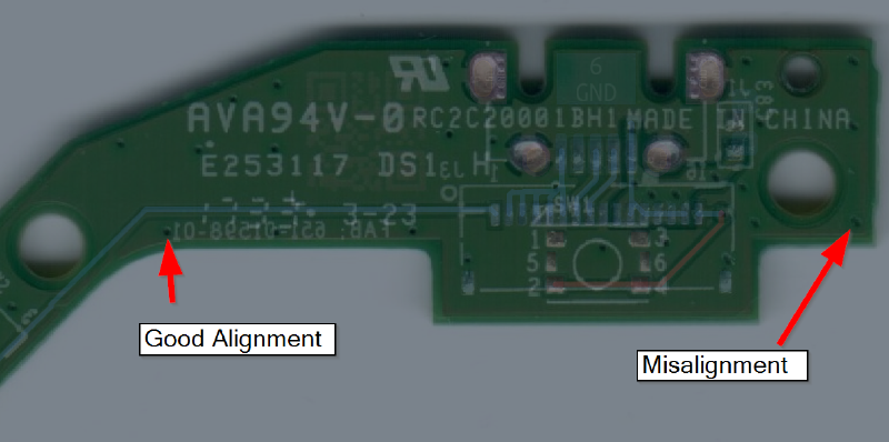
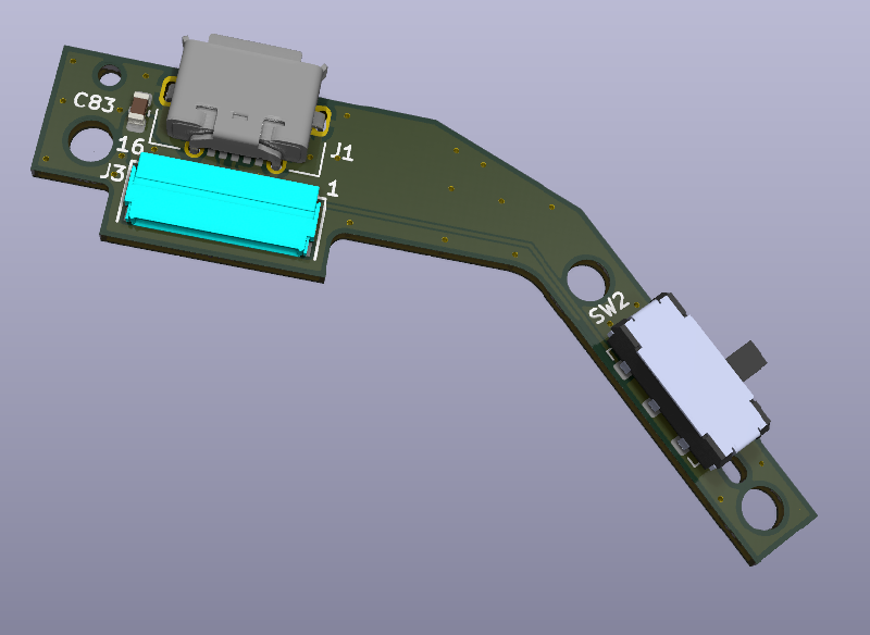
Now that all of the PCB references are in and the parts are in KiCAD, it is just a straightforward tracing operation that I won’t expound upon here.
Conclusion #
At this point I have finished the r1.0 version of the Input PCBA design. Parts have been ordered from Digikey and from PCBWay. The only thing left to do with the input board is to wait, assemble, and fit check.
If you want to follow along with these cloning efforts, check out the Github Repo.
